
Electronic beam evaporation, or e-beam evaporation for short, is a long-used process for producing thin films. High-energy electron beams are employed in this approach to evaporate material from a solid source, which is then deposited onto a substrate in a vacuum. This method is popular in the thin film deposition industry because it is highly accurate and creates uniform coatings.
This blog will go over the working principle, benefits, limitations, and applications of the E-beam evaporation system.
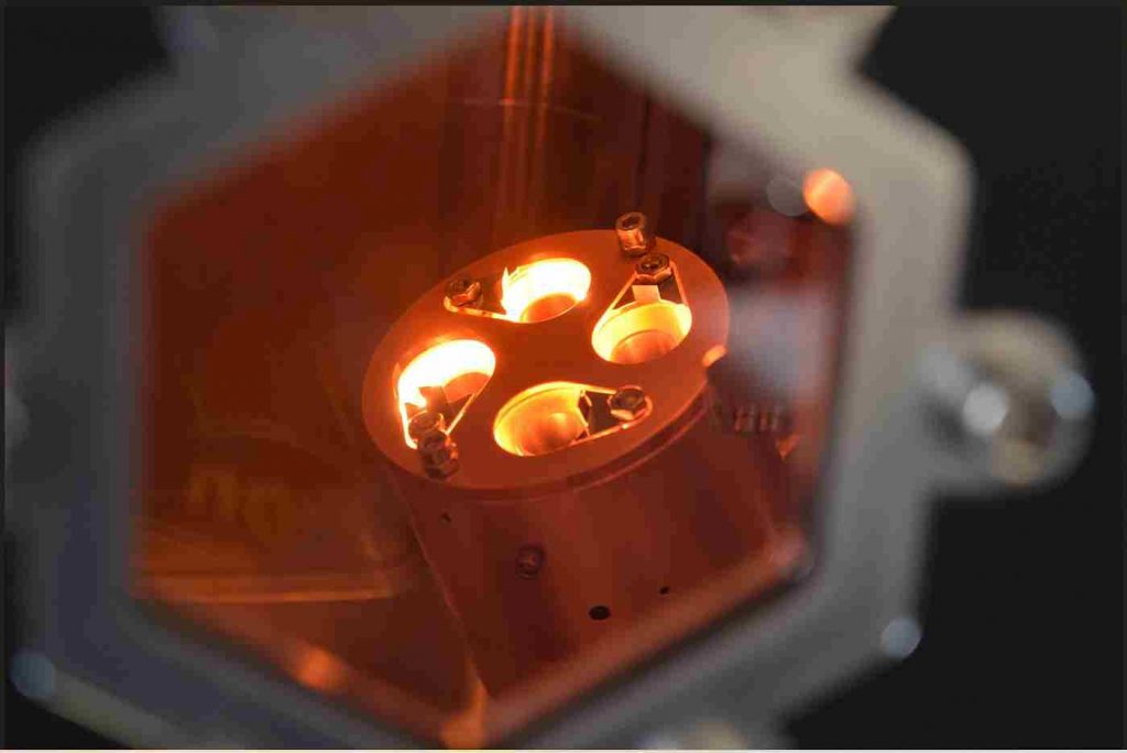
Working Principle of the E-beam Evaporation System
A vacuum chamber, an electron gun, a crucible, a substrate holder, and a power supply are all part of the E-beam evaporation system. The electron cannon fires a high-energy electron beam at the solid source material contained within the crucible. The heat from the electron beam caused the material to evaporate into the vacuum chamber. The substrate holder keeps the substrate in place once it has been covered with evaporated material. The E-beam evaporation system operates in a high-vacuum environment, typically at pressures between 10-4 and 10-6 Torr, to ensure that no external impurities interfere with the quality of the deposited thin layer.
Benefits of an E-beam Evaporation System
The E-beam evaporation system has various features that make it a popular approach for thin film deposition. One of its key advantages is its ability to manufacture high-quality thin films with good adhesion qualities. The high energy of the electron beam ensures that the evaporated material is highly pure and has high kinetic energy, resulting in a thin coating with minimal impurities, high density, and excellent adherence to the substrate.
Another feature of this system is its high deposition rate, which can reach several angstroms per second. This makes it excellent for the deposition of thick films, which can be difficult to achieve with other deposition processes.
The e-beam evaporation system is also a highly controlled process, providing exact control over the thickness and composition of the deposited thin film. The electron beam current and crucible temperature can be changed to prevent the evaporation rate, allowing for the deposition of films with excellent control over their properties.
Limitations of the E-beam Evaporation System
Despite its advantages, the e-beam evaporation technology has certain drawbacks. One of the most significant restrictions is the size of the deposition region, which is usually restricted to a few square centimeters. As a result, it is inappropriate for the deposition of large-area coatings.
Another constraint is the demand for high vacuum conditions, which can be challenging to maintain. This necessitates the employment of specialist vacuum pumps and chambers, which can be costly.
Finally, this technique is not ideal for depositing some materials, such as metals with low melting temperatures, which might result in significant material loss due to thermal evaporation.
Applications for the E-beam Evaporation System
The e-beam evaporation system has numerous uses in diverse industries. In semiconductor manufacturing, e-beam evaporation is extensively utilised for the deposition of thin coatings of metals and metal oxides in constructing semiconductor devices such as transistors and diodes.
In optics, e-beam evaporation creates thin films of dielectric materials such as titanium dioxide, often employed as anti-reflective coatings.
E-beam evaporation is also utilised in the electronics sector to depose thin films of metals, metal oxides, and nitrides, which are employed in manufacturing electronic components such as integrated circuits and magnetic storage devices.
The use of electron beam evaporation to produce 2D materials like graphene and other transition metal dichalcogenides has grown in popularity in recent years. Because of their distinct electrical and optical properties, these materials are potential candidates for various applications. The e-beam evaporation system provides a precise and controllable way for depositing these materials onto substrates, allowing the creation of 2D devices with exact control over their properties.
High-quality, homogeneous coatings are necessary for optimal device performance, which is why the e-beam evaporation method is also used to create thin films for solar cells. Thin-film solar cells, for instance, use e-beam evaporation to deposit layers of silicon and other elements. The e-beam evaporation method is applicable in nanotechnology due to the need for fine-tuned regulation of the deposition procedure. For example, the deposition of thin coatings of nanoparticles onto substrates using e-beam evaporation paves the way for producing devices and materials at the nanoscale that exhibit novel properties.
One can also use the e-beam evaporation method to create medical device coatings. Thin films can be put on medical implants like stents or prosthetic joints to improve biocompatibility, minimise wear, and lengthen lifespan.
What Is the Advantage of Evaporation Over Sputtering?
Sputtering and electron beam evaporation are two physical vapour deposition processes. In electron beam evaporation, a source material is heated by focusing an electron beam on it, whereas in sputtering, ions clash with a target material within a closed magnetic field. Both processes generate thin coatings with low contaminants; however, electron beam evaporation has a faster deposition rate, whereas sputtering is ideal for automation.
Electron beam evaporation is the method of choice for high-volume batch production of thin-film optical coatings. Sputtering, on the other hand, is better suited to applications that demand automation. However, sputtering has fewer uses than electron beam evaporation, which allows for the vaporisation of high-melting-point materials with a short deposition period.
Finally, the unique application requirements determine the best physical vapour deposition method. To achieve the optimum precision, utility, and efficiency in your application, you must examine the strengths and limitations of each technique.
Future E-beam Evaporation System Developments
As technology advances, we should anticipate seeing more advancements in e-beam evaporation processes, broadening their potential applications and capabilities. Recent studies, for example, have focused on using e-beam evaporation to deposit hybrid organic-inorganic thin films, which could have implications in domains such as electronics and photonics.
There has also been an investigation on the use of e-beam evaporation for the deposition of superconducting thin films. This could significantly impact the development of new superconducting gadgets and technology.
Conclusion
Finally, the e-beam evaporation system is a versatile and practical tool for thin film deposition in various industries. It’s a popular choice for many applications due to its capacity to deposit high-quality films with remarkable structural features, good uniformity, and deposit materials with high melting temperatures. As technology advances, we should expect greater advancements in e-beam evaporation technologies, expanding their potential uses and capabilities. The e-beam evaporation system has been and will continue to be essential to technology development in various fields.
Follow Techdee for more!